

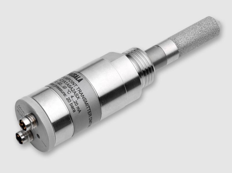
Miniature Dew Point Transmitters DMT143 & DMT143L (Long)
for OEM applications
Technical note
In an earlier article, we discussed measurement solutions for the semiconductor manufacturing process. In this blog, we look at Vaisala’s range of humidity and pressure sensors that ensure accurate measurements for manufacturers of the machines used to produce semiconductors.
In the semiconductor manufacturing process, a whole silicon wafer, or even the whole batch, can be spoiled by even tiny variations in conditions such as temperature, exposure time, chemical concentration, material quality, or contamination. The sources of these variations must therefore be eliminated to ensure a stable and easily replicable process, and measurements used to adjust the various process parameters are key to this. The most important steps in the process of manufacturing silicon wafers are chemical cleaning, lithography, wafer coating and development, wafer expansion and dicing, chip probing and testing, packing, and transportation to the electronics manufacturer.
Vaisala’s measurement solutions for semiconductor equipment vendors are presented below.
The objective of the wafer cleaning process is to remove chemical and particle impurities without altering or damaging the wafer surface or substrate. As most cleaning techniques use chemicals, it is imperative that the measurement sensors are able to tolerate them.
Vaisala humidity sensors have a chemical purge function that frequently heats the sensor element to evaporate chemical pollutants such as solvent vapors, allowing it to survive in chemical-rich atmospheres. The sensor itself is also mechanically protected to resist corrosion, and some instruments are equipped with a heater element that keeps the probe dry while providing real-time dew point calculations. If there is another sensor measuring the actual temperature, relative humidity can be calculated reasonably easily based on the dew point and process temperatures, and most Vaisala instruments are capable of doing this automatically.
After the chemical cleaning process, microstructures are etched on the wafer surface, adding impurities to create a semiconductor structure and oxidize the different insulation layers. The result is several overlapping layers of electrical structures that create, for example, a complex microprocessor chip.
The increasing demand for smaller, lighter components for modern products such as wearables creates a need for more accurate control in the etching process, where optical equipment is used. To produce nanometer-scale structures the exposure must be extremely accurate, as even small variations in ambient pressure, relative humidity, and temperature can alter the optical behavior of the lens. This means that the lens must be adjusted in real time based on these measurements.
The following parameters are essential to improve quality on the stepper that prints the patterns on the silicon wafers: humidity, temperature, and ambient pressure. Meanwhile, the coating and developing machine needs measurements for water in the device drying process.
The Vaisala Indigo520 with Indigo compatible smart probes can be used as an individual humidity instrument, and if several probes are needed it can be combined with the Indigo520 transmitter, which also offers the optional capability of measuring absolute pressure.
Once the semiconductor structures are prepared, the individual chips must be separated from the wafer. There are various techniques for this wafer dicing process, for example using a laser. One important step in the process is controlling dew formation by measuring dew point temperature while the wafer processing tape or dicing tape is peeled off. The semiconductor components are also tested in different temperature conditions to ensure that they meet the required product specifications; different grades are available, including consumer, industrial, automotive, military, and aerospace.
Typically, testing is carried out over the full temperature range starting from –40°C (–40°F) or even lower. When the test is completed and the temperature rises again, there is a risk of condensation on the wafer that can damage the sensitive circuit.
Vaisala offers efficient solutions with easy OEM integration for monitoring the dew and frost points inside the machines used to test individual chips after they are separated from the wafer by dicing. Small probes can be integrated inside a test chamber to provide real-time data according to requirements. The DMT143 is a universal transmitter that is capable of handling a wide range of measurements from –70°C (–94°F) up to 60°C (140°F), and the DMT152 is a special transmitter that is optimized for ultra-dry conditions at temperatures between –80°C (–112°F) and –20°C (–4°F).
for OEM applications
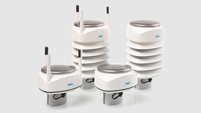
Vaisala Weather Transmitter WXT530 series is a unique collection of cost-effective sensors that accurately and reliably measure weather conditions…
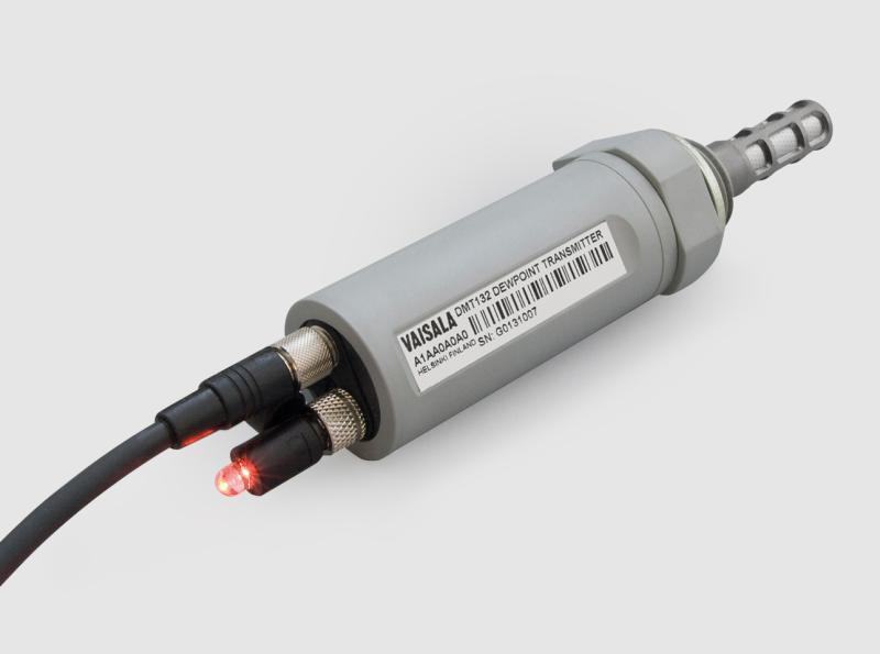
for refrigerant dryers
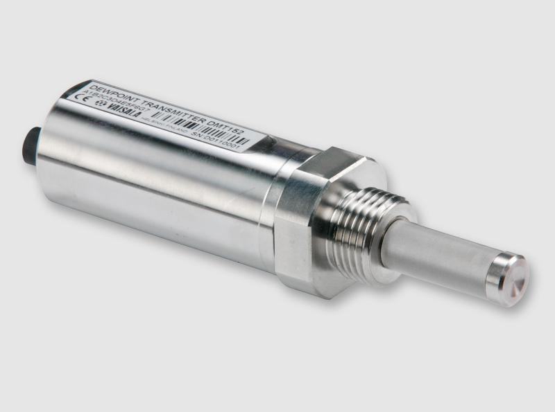
Please note that the DMT152 is being discontinued and should not be specified for new projects. Get to know the new DMT153 here.
For high precision measurements in demanding HVAC applications
with ±1.5%RH accuracy for demanding volume applications
What relative humidity, dew point, absolute humidity and mixing ratio are, how temperature and pressure distort the reading, and why dew point is…
How humidity behaves in real conditions, the three most common measurement problems, and two practical scenarios —heated air and compressed air—…
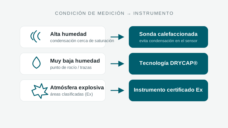
When to measure relative humidity vs. dew point, what high and low humidity demand, how temperature and pressure factor in, and when a warmed probe…

Cooling accounts for up to 40% of a data center's energy demand. This Vaisala guide explains how measurement accuracy cuts costs and risks, with a…
A specialist replies with the solution, the instrument and the service that fit.
Instruments to quote
No instruments yet. An enquiry can be sent anyway: a specialist answers.